
PCB Layout Design Best Practices
2026-09-21 22:58:04 | Donanım Tasarımı | Yazar:Fandou Tech
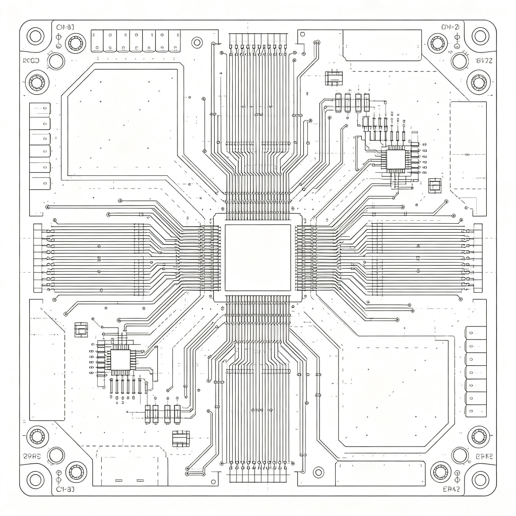
1. Stackup Design
Reasonable stackup design is the foundation of PCB performance, commonly used are 2-layer, 4-layer, 6-layer board designs.
2. Layout Principles
Component layout should follow signal flow, modularization, heat dissipation, anti-interference and other principles.
3. Routing Principles
Routing should consider line width, line spacing, impedance matching, differential pairs, vias and other factors.
4. EMC Design
EMC design includes grounding design, filtering design, shielding design, surge protection and other aspects.